A Mnemonic-less C-Mimicking Assembly Language

Revisiting a self designed Processor Instruction Set. Are its back then innovative [1] Mnemonic-avoiding, [2] C-Mimicking and [3] source, computation destination instruction nature(s) still rare? Still relevant?
1. Introduction
In 1993, Imec Leuven, Belgium asked us, my Masters Thesis mate Ramses Valvekens and myself, to add programmable logic to a CMOS based image chip they developed, called FUGA. Back then image chips in commercial camera’s: camcorders and picture camera’s where usually CCD based. The idea was that IMECs CMOS based image chips had a comparative advantage with respect to CCDs in that the CMOS technology allowed some intelligence to be put on the same chip, since logic is easily put on CMOS but not on a CCD chip. Back in 1993, this was a quite novel idea.
Also, only much later, in retrospect, Bart Dierickx, the CMOS image chip inventor and designer of the FUGA series, thought that this project was probably one of the first to put a full processor as a soft core inside an FPGA. This only became popular many years later.
2. The FUGA Camera Board
IMEC developed a printed circuit board (PCB) that is best described by this specification page.

So from this, you see the Fuge chip has a x address of 8 bits and a y address of 8 bits. This means it has 256 on 256 pixels. It sends back an 8 bit grey level intensity. Note that the grey level is gray-code encoded. This is to avoid that during sampling the output, bits flip and wrong answers are received. It also means our FPGA logic needs to contain a gray encoding to normal binary encoding convertor.
3. The Processor board
We designed a board that was to contain all that expected logic into an FPGA. Of course, apart from the FPGA we needed some peripherals, like pins to program the FPGA via an Xilinx XChecker cable from our PC, some external RAM, a BNC connector to feed the board with a clock, some debugging leds and 7 segment displays to show for example the program counter, a button to step through the program, a serial and parallel interface. So schematically, the board looked like this.

We did not turn this board into a PCB but implemented it as a prototype board and wire wrapped it.
The FUGA chip sat on a separate board, discussed in the previous section. Interconnection between the two boards with a flat cable clicked onto the SC-FUGA connector show in the picture above.
These are two pictures of how our ptototype board looked in real life.

Yes, in black and white still. :) So this being the processor-board, we need to fill the FPGA on it with the processor and some interface logic to the peripherals on the board. The processor requires an instruction set.
4. Processor Instruction Set Design
Rather than adding some limited programmability, via some configurable parameters, or via some macros, we indeed went for the addition of a custom designed full processor.
This processor would then need to be able to:
- read any pixel from the image chip. (The chip had 256 random addressable rows and dito columns. It gave back an 8 bit word representing a grey value that was 0 at the blackest level and 255 at whitest level.
- write to and read from some register set. (We chose b, c, d as 3 8 bit registers, so it could contain any grey level or 8 bit image chip address. Register ‘a’ was chosen as the larger word, so we could accumulate the grey values of a whole image into it, so all 2⁸ * 2⁸ = 2¹⁶ 8 bit words, so maximum the value of 2⁸ * 2⁸ * (2⁸ -1) <= 2²⁴-1 in it. So it needed to be a 24 bits wide ‘accumulator’ register. It’s best to choose register ‘a’ for that because ‘accumulator’ start off with ‘a’. :)
- write to and read from RAM. (We chose the RAM to be structured as a series of image structured portions. So you can apply a RAM address to it, like you can address the image chip. So there is an 8 bit xram and an 8 bit yram address, where you could for example store an entire image, so you could process an image ‘in-place’ in RAM, for example for edge detection or so. Then we added an 8 bit zram address and that then allowed you to have 256 images next to each other. Of course, one can consider the concatenated xram, yram, zram word as one full 24 word RAM address and without thinking about its division in 8 bit parts. :)
- carry out addition and subtraction of gray values; addition for calculating averages, subtraction for comparison of intensities or calibration of images.
- use fixed constants. A user may program something like b+= 2 or b+=5, say in a for loop. Then the constant 2 or 5 needs to come from somewhere. We designed a constant bank of 32 constants to provide for that. The assembler/compiler would have to pick up from the starting code, that if the programmer wrote b+=5, that a constant with contents 5 should be provided, say const9 and also that the line b+=5 would have to be replaced with b+=const9.
- read a program from ROM. Yes, a program has to be stored somewhere. In fact, since we design the whole system in an FPGA, the ROM bits makes is a part of the bit string that is used to program the FPGA.
- execute goto jumps based on no condition or on some conditions. We had chosen to always compare the ‘a’ regsiter with a comp(arator) register and provided jumps depending on equality, non-equality, and larger-or-equal and smaller-than-equal. Rather than inventing quite unintuitive mnemonics, as for instruction set design, was all the rage back then, and in fact still is, we wondered why, and found this better since more easily understood phrases like ‘if(acc!=comp)goto’ and if ‘(acc≤com)goto’ and such.
- read in from and write to a parellel as well as serial interface
- read in the setting from a DIP switch
- write out an internal number to a a 2 7-segment displays
So with all these requirements, and a lot of more fun tinkering and crafting we came to this as the instruction set.
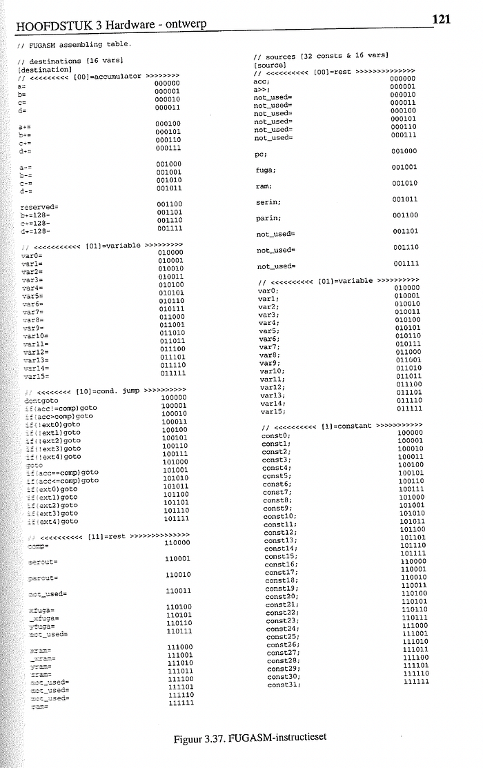
We called this assembly language ‘Fugasm’ as a contraction of FUGA, which was the name of the CMOS image sensor series developed at IMEC in the days and Asm as a contraction of or also commonly used file extension for Assembly language files.
As you can see, there is a division in two columns. A left part, which we call the destination part, and a right part, which we call the source part. Any full instruction is constructed from taking a left part, and a right part. So take b+=128-var3, then this will do b=b+128-var3, as if it was pure C code.
We were quite satisfied with this result, because:
[1] to understand our Fugasm language, and programs written in it, you just need to know C. You do not need to learn any additional assembly language specific cryptic mnemonics. Questions arising for beginning programmers in any other, mnemonic based, assembly languages like, what was the mnemonic again for store: STO or STR?… I wonder why getting rid of menmonics was never done before. Was it a first? Why? Was it a last? Why?
[2] the fact that an instruction could be composed of any left column part with any right columns part, made that it had in fact about 2⁶ * 2⁶ = 2¹² = about 4096 possible instructions. (Some exceptions exist because of the not_used occurrences.) What instruction set has that variety?² And it’s not that you have to remember 4096 instructions, you just have to learn the left column and the right column and you’re done. So that’s only 128 things to remember, and they are very structured and each of them intuitive, meaning one can guess what their meaning is.
Because we implemented the instruction design and the whole instruction decoding logic (in Xilinx XBLOX electronic schematics) needed for that in pretty much the same few days, we had both co-optimised at once. This led to things like: if you define a+= as 000100, it’s intuitive and nicely structured to define b+=, c+= and d+= as well as the sequential words 000101, 000110, 000111 and the decoding of the last two bits in these destination half instruction is straightforward. The prefix 0001 just means the result has to be added to some target register. The suffix of 2 buts just determines which register. So it is a nice separation of concerns and as a consequence, the decoding logic takes in as few bits as possible. Also, from the binary nature of these systems it makes a lot of sense to define 4 registers and not, say 3 or 5. Solving that puzzle optimally or at least efficiently was a lot of fun.
The whole exercise of instruction set definition was informed by marrying:
- what we had as peripherals (image sensor, serial/parallel port)
- the FPGA internal XBLOX library components/resources (RAM (variables), ROM (constants)), multiplexers of n bits, buses of 2^n bits, the computation primitives (addition, subtraction, shifting left and right)
- and what we had as programmability requirements from a user (‘software programmer’) perspective.
This exercise proved to be intellectually and aesthetically satisfying and so was the result, for us, and we also hope, for you. Hence this article.
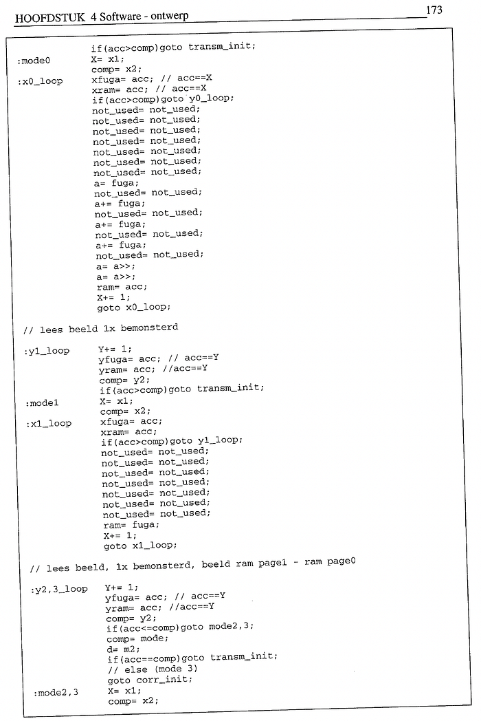
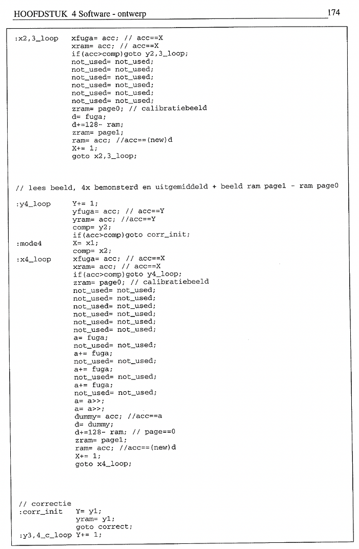
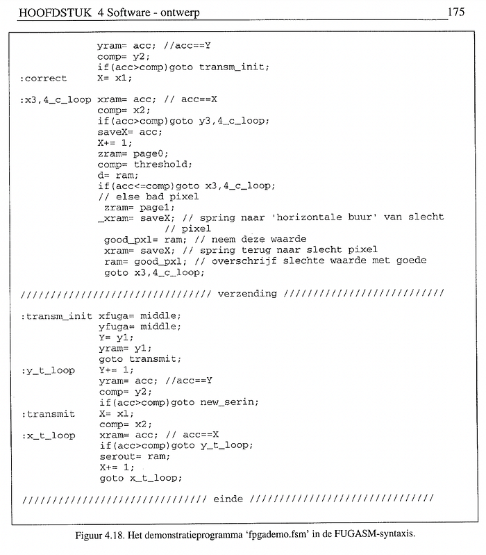
5. Programming in the Fugasm Assembly language
It really looks like programming in C as you will see from the next example program. The program in flow chart form is given in this figure below.
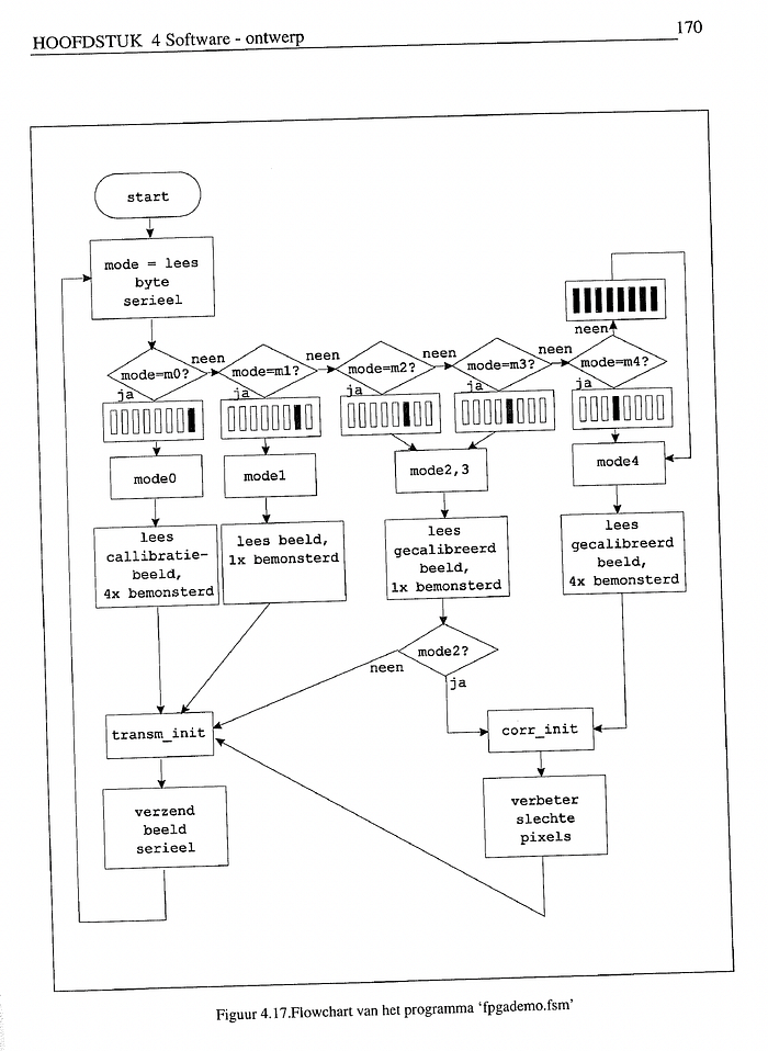
This program reads in the FUGA image. Depending on the mode, which is read from som on board DIP switches, it reads a raw image only, or it reads that multiple time and averages it (to reduce noise to signal ratio), or also subtracts the calibration image from it. A calibration image is made by directing the FUGA camera to an even grey surface. In every case, the resulting image is send over the serial port to a connected PC.
This C-like Fugasm code program looks like this.
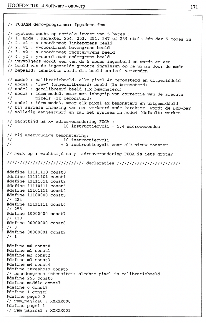
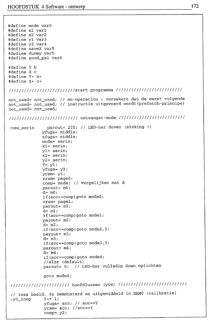
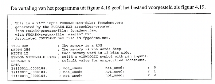
6. The C-Compiler Mimicking Assembler
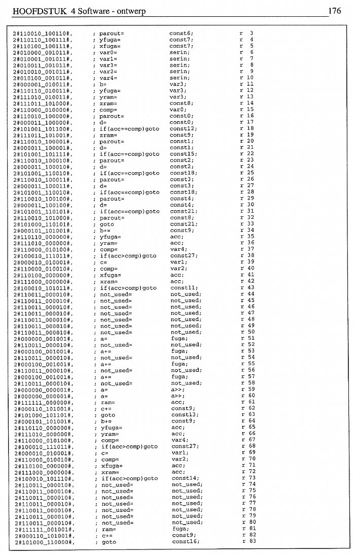
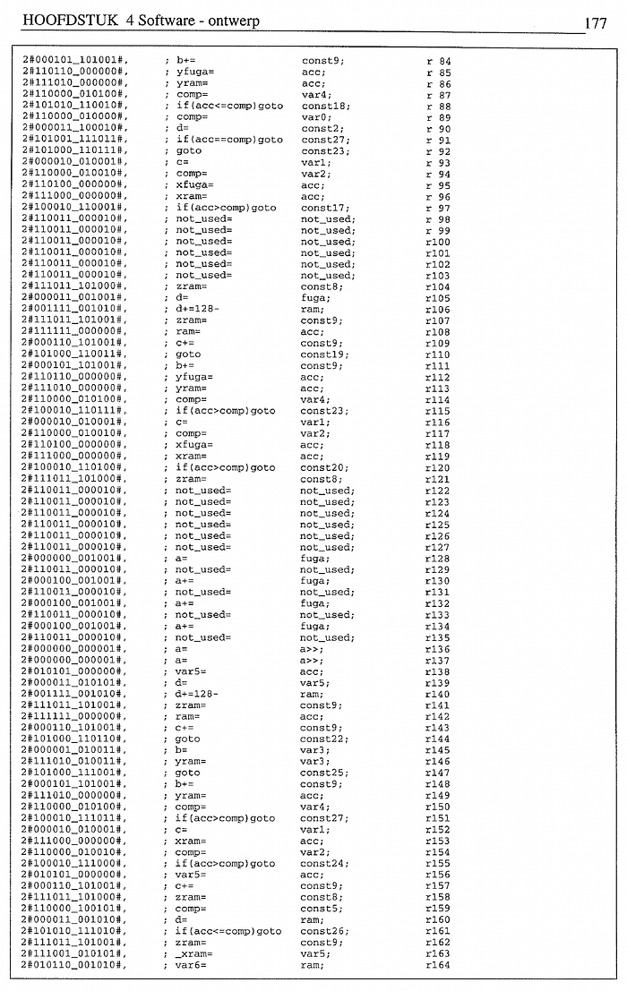
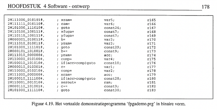
The C-mimicking program above, composed by the user/programmer, is then automatically translated with the assembler to the binary code below.
For documentation, we automatically produce a header that says what source files the generated code has been produced with.
Note that a string like for example: 2#110110_100111# represents a Fugam instruction consisting of the destination 110110, meaning xfuga= and the source 100111, meaning const7, so this instruction assigns the value in constant 7 to the xfuga register.
For back-annotation we also add the original line the programmer has entered as a comments for its corresponding binary instruction.
This then gives the result below.
The constant numbers that the programmer uses directly in his code, together with the constant line numbers where labels are found, are collected and put into a file that is later processed into a ROM block in the design. The ROM description for this program is given here.
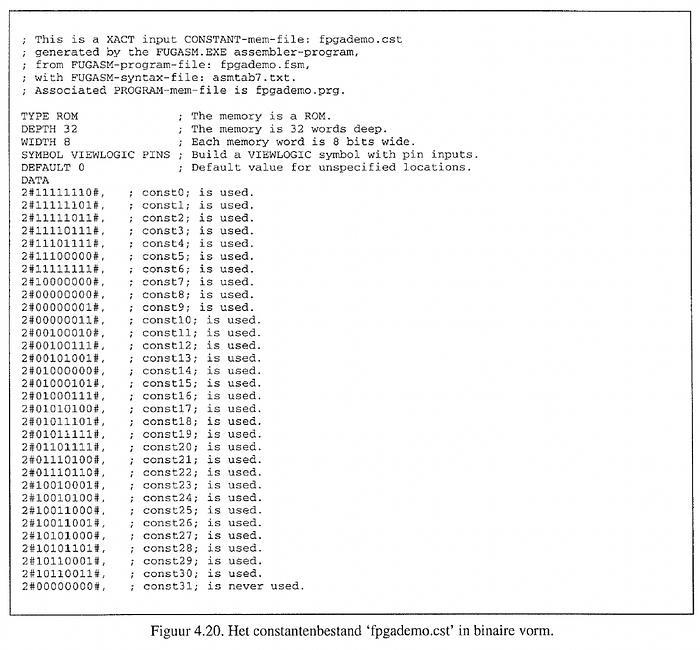
Notice that the ROM block contains up to 32 8 bit words. All but the last one are used here by this program. Constant 7 has value 10000000 here, which the assembler has deduced from the programmer Fugasm statement xfuga = middle; and the preprocessor declaration #define const7 middle. :)
As documentation to the programmer, we defined the FUGASM language in a Backus Naur Form (BNF) file as follows.


This BNF file is only FUGASM language documentation for the programmer to read. We do not need a tool that parses it.
In the above program, you will have noticed that the programmer (me) also has added C/C++ like comments for readability in his code. The parser also has to be able to process this, well to ignore and skip this really. For this it needs a ‘finite state machine’ (FSM) to remember that it is in comment or not in comment state. This looks like this.

Apart from comment and non-comment states, some further states are defined to be able to track where the parser is inside [<binary_number>] strings.
We now designed a language and that assumes a processor that should execute programs in that language. Let’s design that processor.
7. Schematic designs to fill the FPGA
We used XBLOX primitives from the Xilinx library. XBLOX back in 1994 had the then novel feature that you could use primitives with a parameter specifying the bus width of inputs.
We show some examples here.
7.1. Top Level Overview sheet
The overview of the whole collection of interconnected self designed schematic blocks that we put in the FPGA looks like this.

So we have the address busses DEST and SOURCE as well as the DATA bus connecting all main modules. These modules are:
- an ALU for computational tasks on data,
- a CONTROL_UNIT containing a (program) ROM of 256 12 bit instruction words¹ that contains the program,
- a CONSTANT_ROM for constants the programmer has used (either in code directly or as labels to jump to in code),
- a VARIABLE_RAM that contains the registers (inside the FPGA)
- a FUGA interface to read pixel intensities from the FUGA board connected to the flat cable
- a RAM interface to read from and write to RAM chips external to the FPGA but still on the prototype board
- serial_in and serial_out interfaces
- parallel_in and parallel_out interfaces
We select a few of these blocks to discuss.
7.2. Controller sheet
An interesting design part is the ‘controller’ sheet.

As one may expect, it shows how the program ‘COUNTER’ value is used as input into the program ROM (‘PROM’), so that the instruction comes out. One can see and appreciate that the 12 bit wide output ‘ADRESS’ is split via a ‘SLICE’ into a ‘SOURCE’ (6 bit wide) word and into an also 6 bit wide ‘DESTINATION’ word. Also, notice that the (loadable counter XBLOX module) called ‘COUNTER’ contains a ‘LOAD’ 1 bit signal and an 8 bit wide D_in port that can receive a program address and that this comes from a block we designed and called ‘IFGOTO’ block. This is of course the block that decides if a jump to another program line has to be made, in which case the program counter goes there instead of just incrementing with 1.
7.3. Arithmetical Logical Unit (ALU)
As defined by the desired instruction set, we wanted 4 registers a,b,c,d, where each is 8 bit wide, except for the register a wich we want to be 24 bits wide. A high level block diagram is given here.

You will see the central newadder block which contains the real XBLOX addition primitive. It is a 24 bit based one since a is 24 bits wide. When 8 bit addition is done, only the lowest 8 bits are extracted from the 24 bit newadder result. You can see that the result is fed back to the input of the a, b, c, d registers and can be clocked in. Selection of the register defined in the source and destination instruction halves is done by the (‘control enable’) 1 bit signals: CE_a, CE_b, CE_c, C_d. Of course only 1 of them will be active at each time. There are decoded in the ‘address decoder’ from its input source and dest.
The actual implementation of this module in ‘Workview’, the application Xilinx provided for schematic entry design looks a bit more complex.

The separate Workview sheet, for the instruction decoding only, so one more hierarchy level down in the ‘design tree’ of blocks, looks like this.

From this structure, one can appreciate that the source and destination words coming in on the left are decoded by quite simple combinatorial logic and sometimes some additional delaying flip flop or 2 to the 1 bit signals needed on the right. The fact that this logic is ‘simple’ hangs together with a ‘good/consistent/simply structured’ division of the instruction words into subgroups of bits, where each subgroup only steers a selection of functions, like addition or subtraction (the ‘ADD/SUB output signal), or the register selection (the one hot 4 output ‘chip enable’ bits: CE_D, CE_C, CE_B, CE_A) from 2 input bits.
7.4. FPGA Pinout
From all these blocks realised on the inside of the FPGA, results this pinout schema towards the rest of the components on the prototype board.

Assignment of the signals to the pin set available, was also a kind of a fun manual optimisation game. Concerns were to put signals on pins close to the peripherals of the FPGA the signals need to come from or go to. Some pins are reserved for VCC and GND.
This XC4010 FPGA had a ball grid array. Mounting it on a real PCB normally means that all soldering balls need to be melted at the same time and so this would mean advanced soldering method using an oven. Instead, we mounted it in a zero insertion force (ZIF) socket which avoided that we needed to do any soldering at all.
8. Conclusion
The instruction set we designed, in my mind, had 3 quite innovative aspects:
- it avoided mnemonic abbreviations and adapted to more intuitive syntax
- it mimicked the C-syntax (for example the use of the += operator) as such leveraging the biggest programmer community at the time
- from the previous point automatically followed that it combined a source and destination part, resulting in a fetch from anywhere, potential computation and storage anywhere being done in 1 instead of typically two clock cycles
During this 1993–1994 master in EE thesis, we learned system design, computer language design, instruction set design, finite state machine design, schematic entry, parser design and assembler and compiler design basics. Defining and testing all this up to a fully operational system was a lot fun back then, and fun again to revisit now, for old times’ sake. :)
The basic design principles are still valid of course, even if today, digital systems, GPUs, like cloud computing servers and AI systems are much larger, they all still use, the same primitives, probably excluding wire wrapping. ;)
2⁵ years after the facts, we want to thank Bart Dierickx and Ramses Valvekens again for this fun collaboration. :)
—
Epilogue:
Ramses and I later joined the digital ASIC design house Easics (pronounce as ‘easy ks’, stands for ‘Engineering ASICs’), spin off of IMEC, Belgium. ‘Easics 1’ was founded in 1995 by Jan Zegers, Jan Decaluwe, Ivo Vandeweerdt and Dirk Calaerts. Rather than using schematic design, Easics specialised in VHDL (VHSIC hardware description language) based digital design services, implementing in both FPGAs and ASICs. Easics grew to a team of about 35 design engineers. In 2001, Easics was bought by Transwitch. In 2004, Ramses and Steven Coenen did a management buy out. ‘Easics 2’ grew again to a team of more than 40 digital design engineers. In 2024, Easics was bought by Keysight.
—
Footnotes:
¹ “256 words should be enough for anyone!” ;) Of course, the program ROM can be easily enlarged by changing the corresponding XC 4010 FPGA parameter value for it.
² Yes, you could downplay this argument by saying that other instruction sets typically do the same in 2 instructions what we do in 1 instruction, for example a load from memory and then an accumulation of that fetched value into a register. But the thing is that we also do these two things in one clock cycle, so it’s quite clock cycle efficient.